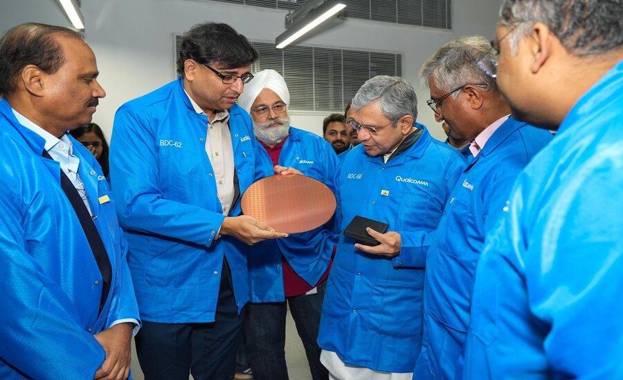
Bengaluru : India has taken a significant step in global semiconductor engineering with the successful tape-out of Qualcomm 2nm chip design at its Bengaluru facility — a development that underscores the country’s growing role in advanced technology design and innovation.
This breakthrough marks a strategic transition from support-based technology work to frontier chip design leadership, contributing to faster performance chips that power devices from smartphones to AI systems.
What Is 2nm Chip Technology and Why It Matters
The term “2nm” refers to the semiconductor manufacturing node size — a measure of the smallest transistors packed onto a chip. A 2nm process packs billions of transistors into tiny silicon surfaces, delivering higher performance, improved energy efficiency, and greater computing power compared with older nodes.
Even though the physical fabrication (manufacturing) of these chips happens at global foundries, the design work being done in India — from architecture to validation — places the country at the centre of future chip innovation.
What Does Tape-Out Mean?
Tape-out is a critical step in semiconductor development. It means that the complete chip design has been finalised and verified and is now ready to be sent for fabrication in a manufacturing plant (fab). This step is significant because design flaws are corrected and the final blueprint of the chip is locked in.
Completing a tape-out at 2nm is especially noteworthy — only a few countries and tech companies are capable of advanced design at such ultra-small nodes.
2nm Qualcomm Chip Design: Qualcomm’s India Engineering Contribution
Qualcomm, a leading global chipmaker, has multiple engineering centres in India — especially in Bengaluru, Chennai, and Hyderabad.
These centres have contributed significantly to the 2nm design:
- Architecture and logic design
- Implementation and verification
- System integration and optimisation
- AI efficiency enhancements
These contributions show India’s strength in high-end chip research and development, rather than just backend tasks.
India has formally launched Qualcomm’s 2 nm semiconductor chip design at an event in Bengaluru
— Defence Decode® (@DefenceDecode) February 8, 2026
▪️2 nm is very advanced chips at this node pack billions of transistors into a tiny area, enabling faster speeds, higher efficiency, and better performance for AI, 5G, edge computing,… pic.twitter.com/Mo9SWbdJpT
Officials have highlighted that India has become one of Qualcomm’s largest engineering hubs outside the United States, reinforcing its importance in global semiconductor workflows.
Government Support and the Semiconductor Ecosystem
At the launch event in Bengaluru, Union Minister Ashwini Vaishnaw emphasised that India is no longer just a support destination but is now involved in end-to-end semiconductor design — from concept to validation and tape-out.
The Government of India’s India Semiconductor Mission (ISM) has further accelerated these developments. Under the new ISM 2.0 plan, priority areas include:
- Chip design and productisation
- Ecosystem partners such as tooling and materials
- Skilled talent development
This policy also supports further growth of research labs, startups, and semiconductor manufacturing units across India.
Importance of 2nm Qualcomm Chip Design
Here is the importance of 2nm Qualcomm chip design;
Technological Credibility – Completing a design as advanced as 2nm firmly places India among countries contributing to next-generation semiconductor innovation.
Economic Growth – As the design ecosystem grows, India is likely to attract more foreign investment, build skilled workforce opportunities, and strengthen its high-tech industry base.
Strategic Advantage – With an increasing demand for AI-capable and edge computing devices, the ability to design world-class chips gives India a competitive technological edge on the global stage.
The Road Ahead
While design is a major milestone, the next challenge will be domestic fabrication (fabs) — which requires high capital, specialised skills, and infrastructure.
Minister Vaishnaw noted that the government is working to build fabrication capabilities, aiming to eventually manufacture chips at advanced nodes within India.
This will help India not only design but also produce next-generation semiconductors in the future.