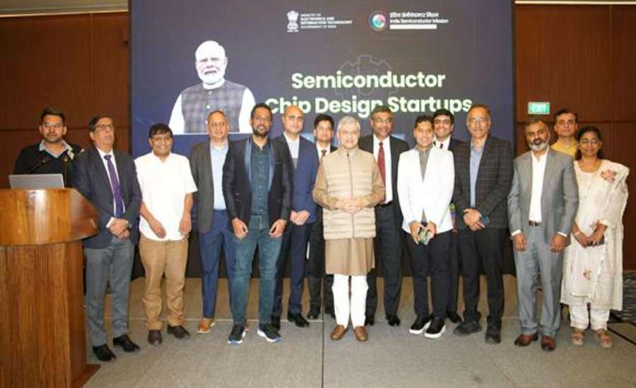
New Delhi: India is moving decisively to become a global hub for semiconductor design innovation under the Design Linked Incentive (DLI) Scheme, a flagship initiative of the Semicon India Programme. Union Minister for Electronics and Information Technology, Shri Ashwini Vaishnaw, met with semiconductor chip design companies approved under the DLI Scheme in New Delhi, highlighting real progress on domestic chip design, strong innovation pipelines, and the government’s long-term commitment to building India’s self-reliant semiconductor ecosystem.
What is the Semiconductor DLI Scheme
Launched as a cornerstone of India’s semiconductor strategy, the Design Linked Incentive Scheme aims to strengthen the domestic semiconductor chip design ecosystem by supporting startups, MSMEs, and academic institutions. The scheme provides financial incentives and access to advanced design infrastructure for the development and deployment of integrated circuits (ICs), system-on-chips (SoCs), chipsets, and other semiconductor IP cores.
Fabless semiconductor design – where companies develop chips without owning fabs – is critical because design and intellectual property contribute a major share of a chip’s overall value. Strengthening this segment reduces dependence on imports, improves supply chain resilience, and accelerates economic growth.
Key Outcomes and Progress under the Semiconductor DLI Scheme
During the interaction, Minister Vaishnaw shared measurable outcomes of the DLI initiative, showcasing how the programme has moved beyond planning to real industry impact:
1. Strong Engagement Across Design Domains
DLI-supported organisations are developing cutting-edge technologies in:
- Compute systems and RISC-V based processors
- RF and networking chips
- Power management and mixed-signal ICs
- Sensors, memory, and AI-enabled low-power chips for edge and IoT applications
- Telecom, automotive, energy, space and defence sectors
These focus areas are highly strategic and foundational to modern electronic systems.
2. Real Chip Outputs and Innovation Metrics
- 122 academic designs taped out, with 56 chips fabricated at 180 nm at Semiconductor Laboratory (SCL), Mohali.
- 16 startup tape-outs, producing six chips at advanced nodes as small as 12 nm.
- Patent activity includes 75 patents from academic institutions and 10 from startups.
- Nearly 2.25 crore tool-hours of usage of advanced EDA tools have been logged, engaging over 1,000 startup engineers and 67,000 trained students.
These metrics show that the DLI Scheme is driving tangible technological outputs, moving India’s semiconductor design capabilities from concept to silicon reality.
From Vision to Reality: Government Support and Strategy
Minister Vaishnaw emphasised that the DLI Scheme’s success stems from a multi-year, ecosystem-driven approach, anchored by a vision outlined by Prime Minister Narendra Modi to transform India into a product-led nation.
Unlike isolated incentives, the DLI Framework provides holistic support across the full design lifecycle, including access to IP libraries, wafer and tape-out support, and advanced design tools. This architecture of support is seen as globally unique and specifically aimed at removing barriers faced by early-stage semiconductor startups.
Scaling Up: Next Phase and Global Recognition
Building on initial success, the government has announced plans to enable at least 50 fabless semiconductor companies in the next phase of the DLI Scheme.
Global industry leaders have taken notice. Feedback shared by the Minister noted a significant shift in international perception—from initial scepticism to enthusiasm for collaborating with India’s growing semiconductor ecosystem. This increased global interest is reflected in venture capital inflows of nearly ₹430 crore into DLI-supported startups, with 14 out of 24 companies already securing funding.
Talent Development and Future Roadmap
A major pillar of India’s semiconductor push is skill development. Against a target of training 85,000 skilled professionals over 10 years, over 67,000 semiconductor professionals have already been trained across more than 315 academic institutions in just four years.
Looking forward:
- By 2029, India aims to design and manufacture chips for 70–75% of domestic applications.
- Under Semicon 2.0, the focus will expand to advanced manufacturing with a roadmap toward 3 nm and 2 nm process nodes.
- By 2035, India aspires to be among the world’s top semiconductor nations.