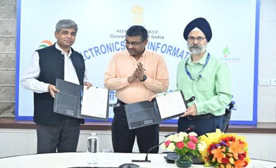
New Delhi: In a major step towards strengthening India’s semiconductor ecosystem and accelerating the objectives of the India Semiconductor Mission (ISM), the National Institute of Electronics and Information Technology (NIELIT) and the Semiconductor Laboratory (SCL), Mohali, have collaborated to make India’s indigenous 1.2 µm Process Design Kit (PDK) available through the national semiconductor education platform eChipHub.
The initiative is expected to significantly expand access to indigenous semiconductor technology by enabling students, researchers, faculty members, startups, MSMEs and industry professionals across the country to design, prototype and develop integrated circuits (ICs) using an Indian process technology.
The collaboration marks another milestone in the government’s broader strategy to build a self-reliant semiconductor ecosystem by combining indigenous technology development, skill creation and industry-academia collaboration.
Indigenous PDK to Strengthen Chip Design Ecosystem
NIELIT, an autonomous scientific society under the Ministry of Electronics and Information Technology (MeitY), has integrated the SCL-developed 1.2 µm Process Design Kit into eChipHub, making it accessible through a secure Aadhaar-authenticated download mechanism.
The move ensures responsible access to indigenous semiconductor technology while encouraging wider adoption among educational institutions, startups and researchers.
The Process Design Kit provides the foundation required for integrated circuit design and fabrication, allowing users to develop chips using an indigenous semiconductor process instead of relying solely on foreign technologies.
What is eChipHub?
eChipHub is India’s national platform dedicated to semiconductor design education and capacity building.
It has been developed under the MeitY-funded project titled “Development of EdTech Platform in Semiconductor Space to Democratize Chip Design and Development Ecosystem for Masses.”
The platform has been jointly developed by NIELIT and SoCTeamup Semiconductors Pvt. Ltd.
Designed as a comprehensive learning ecosystem, eChipHub provides:
- Semiconductor design courses
- Cloud-based virtual laboratories
- Faculty Development Programmes (FDPs)
- Workshops and bootcamps
- Industry internships
- Hackathons
- Academic alliance programmes
- Collaborative chip design projects
Under the ongoing MeitY initiative, NIELIT aims to train nearly 30,000 students in semiconductor design through structured academic and industry-oriented programmes.
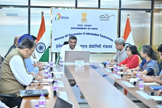
India’s First Indigenous Design-to-Fabrication Learning Pathway
One of the most significant outcomes of the collaboration is the integration of the indigenous open-source Process Design Kit with open-source Electronic Design Automation (EDA) toolchains.
This creates one of India’s first end-to-end indigenous semiconductor design-to-fabrication learning pathways.
Learners will now be able to perform the complete semiconductor design workflow, including:
- RTL design
- Functional simulation
- Logic synthesis
- Physical implementation
- Fabrication-oriented IC design
using an entirely indigenous process technology.
The initiative is expected to reduce dependence on imported semiconductor design ecosystems while nurturing home-grown chip designers and innovators.
Supporting India’s Semiconductor Mission
The collaboration directly supports the goals of the India Semiconductor Mission (ISM) by creating a strong pipeline of skilled semiconductor professionals and encouraging indigenous innovation.
According to NIELIT, the integrated ecosystem will enable students, innovators, startups, MSMEs and academic institutions to convert ideas into fabrication-ready integrated circuit designs using Indian technologies.
Officials believe the initiative will play a crucial role in positioning India as a global hub for semiconductor design, innovation and product development.
Foundation Laid Through 2025 MoU
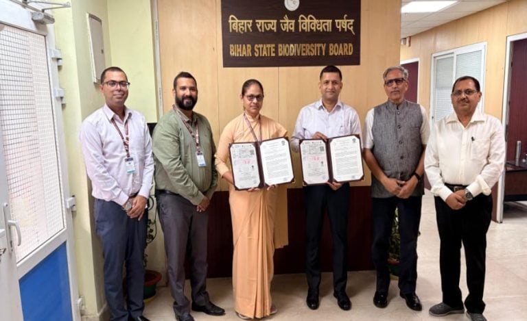
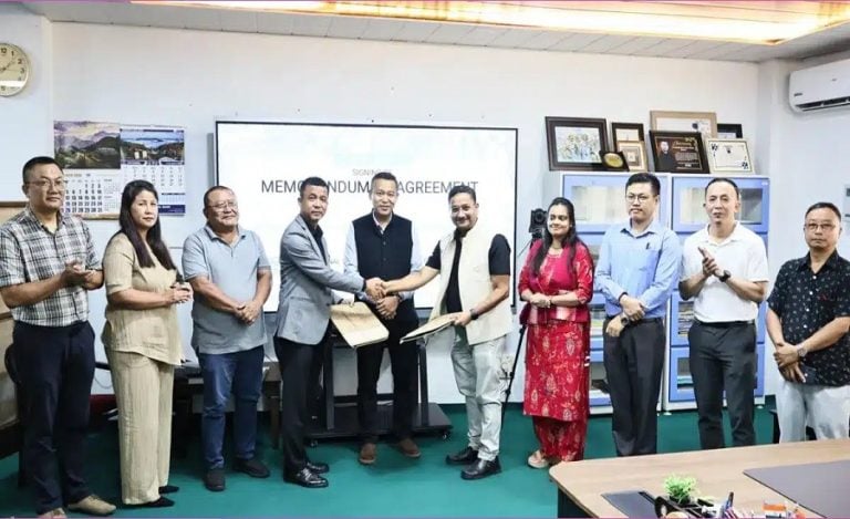
The collaboration builds upon the Memorandum of Understanding (MoU) signed between NIELIT and Semiconductor Laboratory (SCL), Mohali on 25 April 2025 in the presence of MeitY Secretary Shri S. Krishnan.
The MoU aims to promote:
- Semiconductor research and development
- Indigenous technology creation
- Skill development
- Capacity building
- Academia-industry collaboration
- Innovation in semiconductor manufacturing
The current launch of the indigenous Process Design Kit on eChipHub represents one of the first major outcomes of that partnership.
About NIELIT
The National Institute of Electronics and Information Technology (NIELIT) is an autonomous scientific society under MeitY and one of India’s leading institutions for digital skill development.
Its nationwide network includes:
- 56 NIELIT centres
- More than 700 accredited institutes
- Over 8,000 facilitation centres
NIELIT has trained and certified millions of learners in Electronics and Information & Communication Technology (E&ICT).
The institute has also been granted the status of a Deemed-to-be University by the Ministry of Education, with its main campus at Ropar, Punjab, and eleven constituent campuses located across the country, including Aizawl, Agartala, Calicut, Chhatrapati Sambhajinagar, Gorakhpur, Imphal, Itanagar, Ajmer, Kohima, Patna and Srinagar.
Through initiatives like eChipHub and collaborations with organisations such as SCL Mohali, NIELIT is playing a key role in building India’s future-ready semiconductor workforce and strengthening the country’s ambitions of becoming a global semiconductor powerhouse.
About SCL
The Semi-Conductor Laboratory (SCL), located in Mohali, Punjab, is a premier autonomous research institution under India’s Ministry of Electronics and Information Technology (MeitY) dedicated to microelectronics. It serves as a critical asset for national self-reliance, operating an 8-inch CMOS fabrication line and a 6-inch MEMS line at the 180nm technology node to provide end-to-end design, wafer fabrication, packaging, and testing services. SCL has historically supplied specialized, radiation-hardened chips for India’s strategic space and defense sectors, including high-profile missions like Chandrayaan and the Mars Orbiter Mission.
To align with the goals of the India Semiconductor Mission (ISM), the facility is currently undergoing a massive ₹4,500 crore government-backed modernisation drive aimed at upgrading its technology nodes, scaling up commercial production, and transforming the lab into a major hub for domestic chip design, R&D, and talent development.