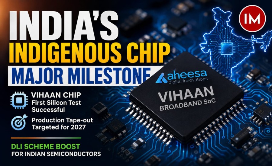
New Delhi: India’s semiconductor design ecosystem has recorded another milestone with Aheesa Digital Innovations’ VIHAAN networking System-on-Chip (SoC) achieving first-pass silicon success. The Chennai-based fabless semiconductor startup is developing the chip for fibre broadband applications, with production tape-out targeted for 2027.
The achievement comes under the Design Linked Incentive (DLI) Scheme, which supports Indian startups developing semiconductor designs for strategic and commercial applications.
VIHAAN Targets Fibre Broadband Applications
VIHAAN has been designed as a networking SoC specifically for fibre broadband. According to the Ministry of Electronics and Information Technology (MeitY), the chip was taped out on Republic Day and achieved first-pass silicon success on Independence Day in 2026.
Read Also: Inside India’s Semiconductor Talent Boom Under the C2S Programme
The chip will now move towards production tape-out, targeted for 2027.
Aheesa, headquartered in Chennai, focuses on semiconductor solutions for broadband networking and security. Earlier this year, the company raised around ₹40 crore from the Tamil Nadu Emerging Sector Seed Fund (TNESSF), managed by TNIFMC, along with other private investors.
DLI-Backed Startups Cross $100 Million in Funding
The government said Aheesa’s progress reflects broader developments in India’s semiconductor design ecosystem.
Key milestones include:
- 455 organisations have received access to advanced chip-design tools, including 350 academic institutions and 105 startups.
- DLI-supported companies have cumulatively raised more than $100 million in venture capital funding.
- These companies have achieved more than 30 chip design tape-outs across different foundries.
- Under the Chips to Startup (C2S) Programme, 245 chip designs have been taped out by 71 academic institutions.
Other DLI-Supported Semiconductor Milestones
The government also highlighted recent developments by other companies supported under the scheme:
- Vervesemi Microelectronics: Achieved first-pass silicon success of a BLDC motor controller chip using an indigenous microprocessor.
- Netrasemi: Successfully tested a 12nm Vision SoC with integrated video analytics acceleration.
- OptoML: Received its 12nm compute-in-memory SoC for faster and more power-efficient AI processing.
- Mindgrove Technologies: Partnered with PRAMA India to explore the use of its Vision SoC in CCTV surveillance cameras.
- IndieSemiC: Secured global certification for its Bluetooth (BLE 6) chip module.
Building a Wider Semiconductor Ecosystem
The government said its semiconductor programmes are aimed at developing capabilities across the wider value chain, including chip design, manufacturing, advanced packaging, equipment, materials, R&D and skilled manpower.
The latest progress comes alongside Semicon 2.0, approved in July 2026 with an outlay of ₹1,27,500 crore.
The government said the growing number of silicon-validated Indian designs indicates that domestic semiconductor companies are moving from chip development and laboratory validation towards production and customer applications.
Read Also: Delhi Semiconductor Policy: CM Rekha Gupta Plans to Transform Capital into Chip Design and R&D Hub