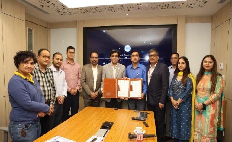
New Delhi: The substrate manufacturing technology in India initiative received a major boost after the Government of Odisha, Intel Corporation, and US-based 3DGS Inc. signed a landmark Memorandum of Understanding (MoU) to establish an advanced semiconductor substrate manufacturing facility in Odisha.
The project is expected to strengthen India’s semiconductor ecosystem, create high-skilled jobs, and support the country’s goal of becoming a global semiconductor manufacturing hub.
According to the official report, this is among the largest high-technology manufacturing investments announced in India.
Odisha-Intel-3DGS MoU: Major Boost for India’s Semiconductor Mission
The agreement was signed in the presence of:
- Ashwini Vaishnaw
- Mohan Charan Majhi
- Lip-Bu Tan
The project aligns with the Government of India’s long-term vision of developing a complete semiconductor manufacturing ecosystem under the India Semiconductor Mission.
What Is the Odisha-Intel-3DGS MoU
The MoU aims to establish an:
- Advanced Packaging Glass Core Substrate Manufacturing Facility
- High-Density Interconnect (HDI) Substrate Production Unit
- Semiconductor Packaging Technology Center
The facility is proposed to be located in the Bhubaneswar-Khurda region of Odisha and will focus on advanced semiconductor packaging technologies. Intel will provide technical expertise, manufacturing know-how, and process support for the project.
Investment Details
Reports indicate that the project could attract an investment of around $3.3 billion (approximately ₹27,000 crore), making it one of the biggest investments in India’s semiconductor manufacturing sector.
Key Highlights
- Estimated investment: $3.3 billion
- Location: Bhubaneswar-Khurda, Odisha
- Technology Partner: Intel Corporation
- Manufacturing Partner: 3DGS Inc., USA
- Implementation timeline: 5–6 years
- Focus: Semiconductor substrates and advanced packaging solutions
Employment Opportunities
The semiconductor project is expected to generate:
- More than 1,800 direct high-skilled jobs
- Thousands of indirect employment opportunities
- Growth in supporting industries such as electronics, logistics, engineering, chemicals, and digital infrastructure
The government believes the project will significantly strengthen the manufacturing ecosystem in eastern India.
Why Semiconductor Substrates Matter
Semiconductor substrates are critical components used in chip packaging and manufacturing. They act as the base layer on which semiconductor circuits and components are mounted.
The Odisha facility will focus on:
- Glass core substrates
- High-density interconnect substrates
- Advanced semiconductor packaging technologies
These technologies are essential for next-generation AI chips, data centers, high-performance computing systems, smartphones, and automotive electronics.
Odisha-Intel-3DGS MoU: Government’s Statement
Union Minister Ashwini Vaishnaw said investments by leading global semiconductor companies show growing confidence in India’s semiconductor sector.
He noted that recent investments and partnerships involving companies such as Applied Materials, Lam Research, Tokyo Electron, Merck Electronics, Tata Electronics, and ASML reflect trust in India’s policy framework and semiconductor ambitions.
How Odisha-Intel-3DGS MoU Supports India’s Semiconductor Goals
The project is expected to:
- Reduce dependence on imported semiconductor components
- Strengthen India’s supply chain resilience
- Promote export-oriented manufacturing
- Build advanced chip packaging capabilities
- Position Odisha as a global semiconductor manufacturing destination
Industry experts believe the facility could become a key part of India’s growing semiconductor value chain.
What is the Importance of Odisha-Intel-3DGS MoU
For Odisha, the project could bring:
- Large-scale industrial investment
- Technology transfer from global semiconductor leaders
- Development of skilled workforce
- Growth in digital infrastructure
- Increased foreign direct investment opportunities
The state government has been actively promoting Odisha as a destination for electronics and semiconductor manufacturing.