New Delhi: Semicon 2.0 has received Union Cabinet approval, marking a major step in India’s plan to become a global semiconductor hub. The government has approved a total budget of ₹1,27,500 crore to strengthen chip design, manufacturing, research, talent development, and supply chains. The policy aims to build a complete semiconductor ecosystem and reduce India’s dependence on imported chips.
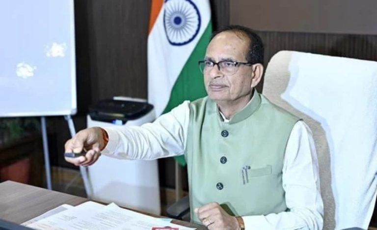
The decision was approved by the Union Cabinet chaired by Prime Minister Narendra Modi on July 15, 2026. The new programme builds on the progress made under Semicon India 1.0 and focuses on long-term growth of India’s semiconductor industry.
What is Semicon 2.0
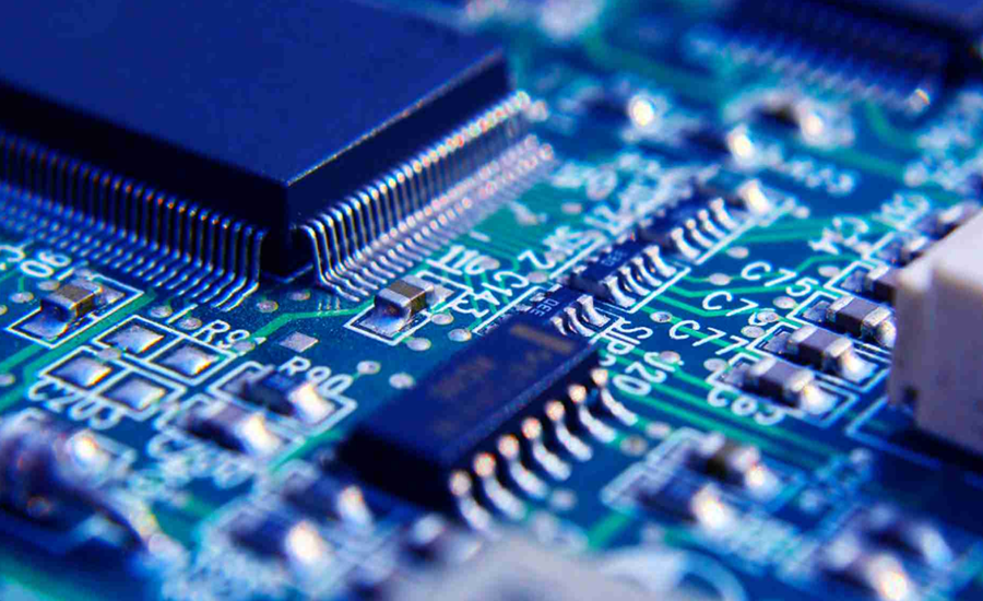
Semicon 2.0 is the next phase of India’s semiconductor mission. It is designed to support every important part of the semiconductor value chain, from chip design to manufacturing and skilled workforce development.
Read also: What is V2V Communication Technology? and How It can Boost Road Safety in India
The government wants India to become a trusted global destination for semiconductor production while improving supply chain resilience and technological self-reliance.
What are the Six Key Pillars of Semicon 2.0
1. Chip Design
The government will strengthen India’s chip design ecosystem by supporting startups and developing Indian intellectual property (IP). The focus will be on designing complete semiconductor chips and systems, helping India become a global centre for semiconductor design.
2. Semiconductor Machines and Materials
Companies manufacturing semiconductor equipment, chemicals, gases, and raw materials will receive incentives. This will help create a stronger domestic supply chain and reduce dependence on imports.
3. More Semiconductor Fabs
India plans to attract additional semiconductor fabrication plants (fabs), including silicon fabs, compound semiconductor fabs, display fabs, and discrete component fabs. The first semiconductor fab is expected to begin operations in 2028.
4. Stronger ATMP/OSAT Industry
The policy will further strengthen India’s Assembly, Testing, Marking and Packaging (ATMP/OSAT) sector. The government aims to attract advanced packaging technologies as global companies look for alternative manufacturing locations.
5. Research and Development
Semicon 2.0 will encourage advanced semiconductor research beyond the current 28nm-110nm technology. Indian institutions will work with leading research centres in India and abroad to develop next-generation semiconductor technologies.
6. Talent Development
Around 315 universities are already training students using industry-standard Electronic Design Automation (EDA) tools. More focus will be given to clean room training, fab construction skills, and advanced semiconductor education to prepare a skilled workforce.
Progress Under Semicon India 1.0
The government highlighted several achievements under the first phase:
- 12 semiconductor manufacturing projects approved with investments exceeding ₹1.64 lakh crore.
- Projects include one silicon fab, one silicon carbide fab, one gallium nitride Micro LED fab, and nine packaging units.
- Companies like Micron, Kaynes, and CG Semi have already started or are preparing for commercial production.
- 24 chip design projects have received financial support.
- 105 startups and MSMEs have received access to professional EDA tools.
- Around 68,000 students have already been trained in semiconductor design.
What is the Importance of Semicon 2.0
Semiconductors are the backbone of smartphones, computers, electric vehicles, telecom equipment, defence systems, medical devices, and artificial intelligence.
A strong domestic semiconductor industry will improve India’s manufacturing capability, strengthen national security, create high-quality jobs, and reduce reliance on imported chips. It will also support the country’s long-term vision of becoming a global technology and electronics manufacturing hub.
Read also: India Unveils NIDAR 2.0: MeitY Pushes Indigenous AI Drone Technology with VEGA Chips